Summary
This paper presents a new non-PFAS (environmentally safer) photo-imageable dielectric material designed for RF silicon interposers. The material offers low dielectric loss, good patternability, and high reliability—important properties for high-frequency communication systems. The authors detail process development, including curing conditions, film quality, and RF performance testing, showing the material's strong potential as a next-generation interposer dielectric.
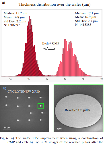
Figure 6 – Wafer Thickness Distribution & SEM Revealed Cu Pillars
Key Concepts
- Non-PFAS materials for environmentally safer RF packaging.
- Low dielectric loss for high-frequency signal integrity.
- Photo-imageable patterning for fine interconnect features.
- Reliability and RF performance under standard test conditions.
RF Performance Considerations
The dielectric constant and loss tangent directly impact insertion loss and signal integrity in RF interposers, making careful material selection critical.